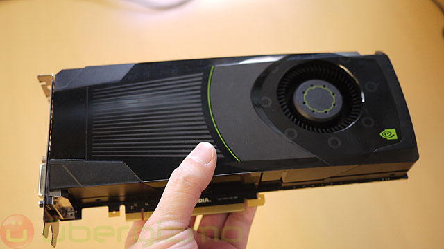
NVIDIA GeForce GTX 680: Great In Every Way

Three times as many cores?!
Yes, you read that right, the latest GeForce GTX 680 features three times as many cores as the previous GeForce GTX 580, thanks to its new SMX multiprocessor block. NVIDIA has been able to add that many cores, by removing some of the chip logic (thread management…) to the software driver. With the newly freed surface area on the chip, NVIDIA is then able to more compute capacity… Computing cores are very dense blocks that pack a lot of computing power, so exchanging thread management logic for computing logic lays the foundation for a much higher compute-efficiency (per square mm).
More importantly, because the GeForce GTX 680 has more cores, NVIDIA is able to reduce their clock so that each of them works “less”, while still achieving better performance as a group. This is really the key to achieving power-efficiency (more on that in a minute). The chip also uses a 256-bit bus (vs. 384 for the GTX 580), but faster memory (6GHz vs 4GHz). Finally, the number of texture units has been doubled (128 vs. 64) to accommodate 3X as many cores to “feed”. Overall, this is a considerable architectural shift.
One (variable) clock to rule them all:
NVIDIA has radically changed the way cores are cadenced. It used to be that different parts of the chip are cadenced by different clocks (in MHz, called “clock domains”). It’s great for some things, but it is difficult to time/orchestrate all those parts that are effectively moving at different speed. That’s particularly true if you want to have a variable clock because graphics processing is basically a very long pipeline, or assembly line for data.
With a single clock domain, NVIDIA is able to increase, or decrease, the chip’s frequency to either boost performance – or save power. We’ve seen the chip go as low as 325Mhz, or as high as 1123Mhz. We’ve been told that board partners can (and will) propose products that go well beyond this upper limit. You can still overclock and tweak things, but now, the large majority of users who don’t want to look into that can also benefit from overclocking, automatically.
The software integration is particularly interesting because the user can choose to tweak performance based on speed (in FPS) or temperature. For example, if you don’t care for frame rates higher than 60FPS (or 30FPS) in games, the GPU will lower its clock to achieve this performance. This saves a ton of power. On the other hand, you could also aim for a temperature limit, and the GPU will go as fast as it can, but without getting hotter than a certain threshold. Your lap will thank you.
TXAA: high-quality, high-performance Anti-Aliasing
If you’re a GPU enthusiast, you probably are very familiar with anti-aliasing, a technique that removes “jaggies” from rendered images. It’s very well known that cranking AA up can quickly bring performance down. The default AA modes in DirectX would do that easily. To address this, NVIDIA has come up with TXAA (an upgrade from FXAA), an anti-aliasing mode that can basically double the performance while maintaining the image quality. It should be very easy for developers to use this, and a number of titles should already feature it at launch.
It gets even better with laptops
Everything that we mentioned earlier is very important for laptops because the GPU has the potential of consuming so much power if the frequency is not throttled. Now, it is possible for the GPU to scale between extreme performance and extremely low clock speeds. Finally, for mundane tasks, it is always possible to fall back on the integrated graphics and shut down the GPU completely with the NVIDIA Optimus feature.
Conclusion
With the GeForce GTX 680, NVIDIA easily captures the top spot for being the fastest single-chip graphics processor, and does so in an elegant way by keeping pricing steady while lowering thermal and power requirements significantly. In many ways, this is a perfect product from a chip-making standpoint. Actual in-game performance will vary on each game: for example, the GeForce GTX 680 does very well in Battlefield 3 or Dirt 3, but so no much in Crysis: Warhead. However, at the end of the day, it is still a clear win for the GTX 680.
You May Also Like
Popular Right Now
- Flappy Bird Is Back! After 10 Years, It Brings A New Game Experience
- Google Messages Rolls Out On-Device Nudity Detection With Sensitive Content Warnings
- Google AI Mode Adds Multimodal Search To Mobile App
- Leaked Apple Watch Series 10 Prototype Reveals Unique Health Sensor And Potential Future Features
- Canon Unveils PowerShot V1 And EOS R50 V: Best New Vlogging Cameras For 2025
- Bill Gates Predicts: AI Will Replace Doctors And Tutors Within A Decade
- First Shutdown of Niagara Falls in 12,000 Years: A Rare Sight to Behold
- Former Google Engineer claims that humans will achieve immortality soon
- Romotow: The Foldable Camping Trailer Inspired By A USB Flash Drive
- LYRA: Swiss Startup Unveils AR Smart Glasses for Office Work, City Life, And Traveling
- Man Caught in China Smuggling $46K Worth of Intel CPUs Wrapped Around His Waist
- iPhone 15 Pro Max may bring thinner bezels than Xiaomi and Samsung’s latest flagships
- OpenAI's new GPT-4 with a "human-level performance" scored up to 93% on SAT exams
- iPhone SE 4 could be Apple's secret weapon to 'steal' budget customers from Samsung
- Lenovo Launches New Workstations, With Aston Martin DNA
- Ubergizmo’s Best of Mobile World Congress 2023